KAIST
BREAKTHROUGHS
Research Webzine of the KAIST College of Engineering since 2014
Spring 2025 Vol. 24Quantum Jumping Quantum Mechanical 2D Device Simulations
Developing an alternative to the standard theory of quantum transport, a new simulation approach has been established for atomically-thin two-dimensional (2D) nanodevices in operando conditions. The approach for the first time allows faithful, first-principles modeling of graphene electrode-based 2D tunneling devices.
Article | Spring 2023
With the continued miniaturization of semiconductor chips to atomic scale, there has been an increased demand for development of better theory and simulation tools to design nanoscale devices. Prof. Yong-Hoon Kim and his group from the KAIST School of Electrical Engineering have developed a novel theoretical approach to predict quantum transport processes in nanodevices under finite bias and/or gate voltage conditions. Using computer software to implement the formalism, the team has been the first to successfully calculate the finite-bias operation behavior of graphene electrode-based 2D tunneling transistors in a first-principles manner.
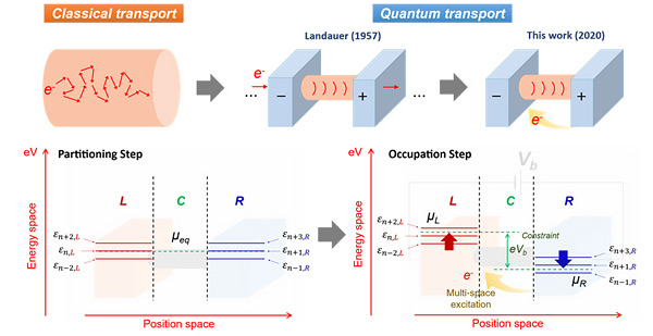
Based on density functional theory (DFT), for which the 1998 Nobel Prize in Chemistry was awarded to physicist Walter Kohn, first-principles material simulations are now widely and routinely performed. In contrast to the simulation of materials in equilibrium, first-principles schemes to treat nanoscale devices in nonequilibrium have emerged only recently. The current state-of-the-art approach is to combine DFT and nonequilibrium Green’s function (NEGF) formalisms within the Landauer picture. However, this scheme suffers from several theoretical and technical shortcomings, which are particularly significant for recently-emerged yet scientifically and technologically important atomically thin two-dimensional (2D) devices.
To understand this background, it should be stressed that understanding and controlling nanoscale electrical current flow is at the heart of research and development of nanoelectronic devices. While electrical current flow at the macroscale had been conventionally understood in terms of response to an applied electric field, Landauer in 1957 presented another viewpoint that is more suitable at nanoscale. In the Landauer picture, current flow is either seen as the outcome of the charge inflow/outflow at the channel-electrode boundaries, or the device is seen as a system in which a channel in nonequilibrium is sandwiched between two semi-infinite electrodes in equilibrium (Figure 1 top panel). The many-body NEGF theory and Landauer picture has now become the standard computer simulation scheme for nanoscale devices. However, the requirement of semi-infinite electrodes is a serious bottleneck in simulating 2D heterojunction devices such as tunneling transistors, which are made by sandwiching several hexagonal boron nitride (hBN) layers between graphene electrodes. Prof. Kim’s group has demonstrated that atomically-thin 2D devices can be faithfully modeled if an alternative viewpoint for quantum transport is adopted in which quantum transport is mapped to the drain-to-source or multi-space electronic excitations (Figure 1 bottom panel).
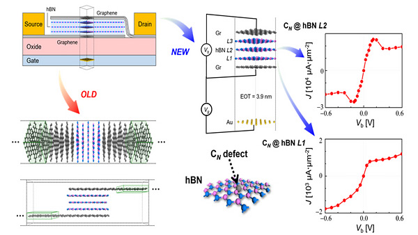
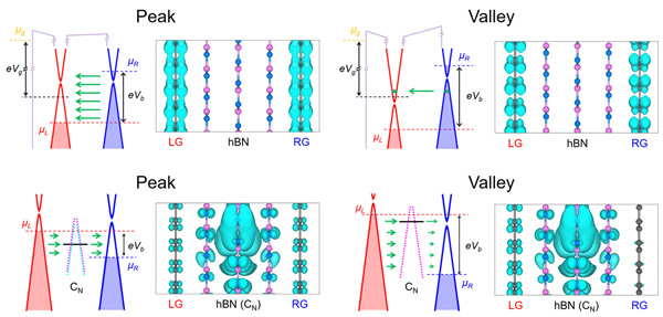
Based on the newly-developed formalism, Prof. Kim’s team termed as multi-space constrained-search DFT (MS-DFT), the team studied graphene/several-layer hBN/graphene heterojunction 2D tunneling transistors (Figure 2). This device’s architecture has been experimentally realized and promising device characteristics such as chiral quantum state, giant tunneling magnetoresistance, and negative differential resistance (NDR) have been reported. However, due to the theoretical difficulties in handling the laterally periodic 2D device geometry (Figure 2 left panel), most theoretical studies so far have resorted to semi-classical approaches, eliminating the possibility of interpreting and predicting effects that involve atomistic details in an ab initio manner. Indeed, the MS-DFT simulations demonstrate that the presence of atomic defects can strongly affect device characteristics. In particular, considering that a carbon atom was substituted for a nitrogen atom (CN), the team showed that an atomic defect can become the origin of experimentally-observed nonlinear NDR current-voltage characteristics depending on its location within the hBN channel (Figure 2 middle and right panels). This NDR mechanism contrasts with the standard NDR mechanism that involves electrostatic gating effects, and the team explained that it belongs to a class of novel “quantum-hybridization NDR” mechanism that was discovered several years ago by Prof. Kim’s group (Figure 3). Overall, this breakthrough points toward a future of computer-aided design of nanoscale semiconductor devices.
More information: Tae Hyung Kim, Juho Lee, Ryong-Gyu Lee, and Yong-Hoon Kim, “Gate-versus defect-induced voltage drop and negative differential resistance in vertical graphene heterostructures” Npj Comput. Mater. (2022) DOI: 10.1038/s41524-022-00731-9; Juho Lee, Hyeonwoo Yeo, and Yong-Hoon Kim, “Quasi-Fermi level splitting in nanoscale junctions from ab initio”, Proceedings of the National Academy of Sciences of the USA (2020) 10.1073/pnas.1921273117; Juho Lee, Han Seul Kim, and Yong-Hoon Kim, “Multi-space excitation as an alternative to the Landauer picture for non-equilibrium quantum transport”, Advanced Science (2020) DOI: 10.1002/advs.202001038.
Most Popular

When and why do graph neural networks become powerful?
Read more
Smart Warnings: LLM-enabled personalized driver assistance
Read more
Extending the lifespan of next-generation lithium metal batteries with water
Read more
Professor Ki-Uk Kyung’s research team develops soft shape-morphing actuator capable of rapid 3D transformations
Read more
Oxynizer: Non-electric oxygen generator for developing countries
Read more