KAIST
BREAKTHROUGHS
Research Webzine of the KAIST College of Engineering since 2014
Fall 2025 Vol. 25Programmable photonic integrated circuits with extremely low-power consumption

Researchers at KAIST and DGIST have developed programmable photonic circuits with extremely low power consumption and reconfiguration energy, based on microelectromechanical systems (MEMS) technologies.
Researchers at KAIST and DGIST in Korea have developed programmable photonic circuits with extremely low power consumption and reconfiguration energy, based on silicon photonics and microelectromechanical systems (MEMS) technologies. The photonic circuits use two fundamental optical elements, tunable couplers and phase shifters, with capacitive MEMS actuators to offer unique advantages over conventional thermo-optic approaches in a variety of classical and quantum photonics applications.
The MEMS-tunable couplers and phase shifters allow for precise control of optical signals, with a single-element standby power consumption of less than 10 femtowatts and reconfiguration energy of only 40 picojoules at maximum. These are the lowest static power and tuning energy ever reported for densely integrated programmable photonic circuits. The circuits have potential for use in a range of applications, including photonic neural networks, quantum photonics, and RF signal processing. Due to their low power consumption, the technology is highly scalable, with potential for chip-scale programmable photonic integrated circuits.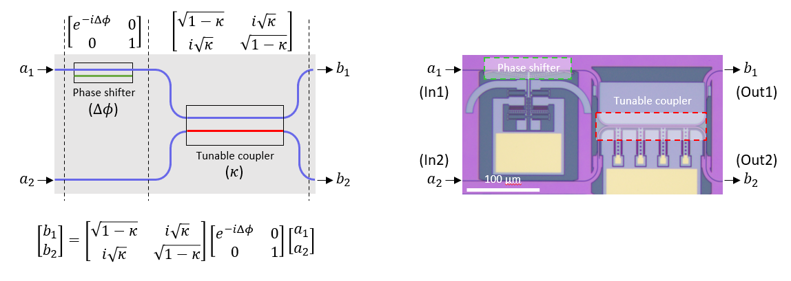
"This research represents a significant step forward in the development of programmable photonic circuits," said Prof. Sangyoon Han at DGIST, a corresponding author of the paper. "The use of MEMS technology allows for highly-scalable reconfigurable photonic circuits with low power consumption and reconfiguration energy, making them ideal for a wide range of applications in photonics."
This technology has the potential to transform several industries, from data communications to computing and beyond. "We believe that this technology can also be applied to process quantum information," said Prof. Kyoungsik Yu at KAIST, another corresponding author of the paper.
The research was conducted by a team of researchers at KAIST and DGIST in South Korea, with the support of the Samsung Research Funding & Incubation Center of Samsung Electronics and the National Research Foundation of Korea. The team is working on further developing these programmable photonic circuits, to make the circuits even more efficient and scalable in the future. Their findings have been published in Nature Photonics.Most Popular

A New solution enabling soft growing robots to perform a variety of tasks in confined spaces
Read more
Development of a compact high-resolution spectrometer using a double-layer disordered metasurface
Read more
Towards a more reliable evaluation system than humans - BiGGen-Bench
Read more
AI-Designed carbon nanolattice: Feather-light, steel-strong
Read more
Dual‑Mode neuransistor for on‑chip liquid‑state computing
Read more