KAIST
BREAKTHROUGHS
Research Webzine of the KAIST College of Engineering since 2014
Spring 2025 Vol. 24Efficient interface for tiny nanolasers
KAIST researchers propose a highly efficient coupling interface for metal-optic nanolasers using metal slot waveguides.
Article | Spring 2015
For high-density photonic integrated circuit applications, significant advances have been recently made in realizing nanoscale optical circuits capable of routing and manipulating light waves beyond the traditional diffraction limit, which has dictated that the electromagnetic waves are not allowed to be squeezed into the regions much smaller than their wavelength. Pursuing light sources that can drive such optical circuits, many researchers have investigated the design, fabrication, and characterization of subwavelength-scale devices because of their small physical size, low power consumption, and energy efficiency.
Because of diffraction, however, light output emanating from tiny structures diverges quickly, and it is not trivial to establish an efficient connection between such light sources and optical waveguide circuits. One of the important next steps in this development is, therefore, the realization of an efficient coupling scheme that can funnel the light output from the tiny light sources into the passive optical waveguide circuitry for more complicated applications such as chip-scale optical interconnects. Interestingly, few studies have been reported on such coupling interfaces due to various practical and fundamental issues.
Prof. Kyoungsik Yu’s research group at the department of electrical engineering at KAIST proposed the surprisingly simple idea of using the metal slot waveguide guide — the light propagates within the gap space between the metal block — as a highly efficient coupling scheme for the subwavelength metal-patch-type nanolaser that consists of metal-semiconductor-metal layers. Based on efficient evanescent wave coupling and mode matching, the metal slot waveguides can efficiently transfer the electromagnetic energy to/from the metal-patch cavity without greatly affecting the important optical properties, as schematically illustrated in the image. They also support the strong subwavelength-scale confinement of the propagating optical waves with reasonable propagation losses. In addition, by taking advantage of the resonant properties and strong light localization, KAIST researchers also suggested multi-port optical filters, which are one of the essential components in optical signal processing and multi-channel communications to select/reject particular wavelength components.
This work was selected as a recipient of a gold medal for the best poster award of the NanoKorea 2014 symposium in August 2014.

Most Popular

When and why do graph neural networks become powerful?
Read more
Smart Warnings: LLM-enabled personalized driver assistance
Read more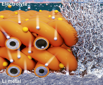
Extending the lifespan of next-generation lithium metal batteries with water
Read more
Professor Ki-Uk Kyung’s research team develops soft shape-morphing actuator capable of rapid 3D transformations
Read more
Oxynizer: Non-electric oxygen generator for developing countries
Read more