KAIST
BREAKTHROUGHS
Research Webzine of the KAIST College of Engineering since 2014
Spring 2025 Vol. 24Three-atom-thick semiconductor for future electronics
A scalable method to prepare an atomically-thin layered semiconductor was developed.
Article | Fall 2015
Great efforts have been made to achieve fast, high-performance electronics by reducing the dimensions of devices, which were characterized by Moore’s Law, stating that the number of transistors in IC doubled every two years. However, such efforts are now facing limitations since the properties of silicon – a primary constituent of modern electronic devices – greatly deteriorate when scaled down to few nm due to the quantum confinement effect.
Fortunately, two-dimensional (2D) transition metal dichalcogenide (TMDC) crystals stacked by weak van der Waals interactions can overcome this problem. Having high mobility at thicknesses of a few atoms with >106 on/off ratio, TMDC crystals’ high flexibility and mechanical strength and low susceptibility to scaling make them as a good candidate to replace silicon in technologies. However, the scalable growth techniques for industrial applications are still not well-established.
In a recent paper published in ACS Nano, a research team led by Prof. Sung-Yool Choi (EE) solved the problem by utilizing the chemical vapor deposition (CVD) method. The process they proposed makes use of a simple reaction between selenium and molybdenum (VI) oxide precursor at the vapor phase and is applicable to a large area on any substrate such as graphene, sapphire, and SiO2 substrates. Interestingly, the team found that the physics at the semimetal-semiconductor junction coming from GR-MoSe2 is different and revealed that the time-scale of the charge transfer at the hetero-interface is much smaller than that of intralayer excitonic recombination, suggesting that manipulation of charge carriers in 2D systems is possible with ease and that it can be further applied to design highly effective photodetectors, solar cells, etc.

Most Popular

When and why do graph neural networks become powerful?
Read more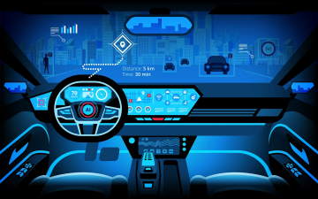
Smart Warnings: LLM-enabled personalized driver assistance
Read more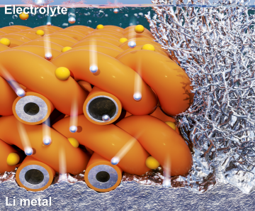
Extending the lifespan of next-generation lithium metal batteries with water
Read more
Professor Ki-Uk Kyung’s research team develops soft shape-morphing actuator capable of rapid 3D transformations
Read more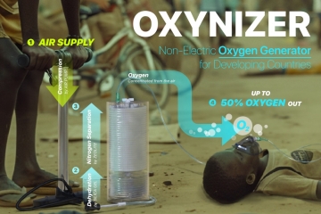
Oxynizer: Non-electric oxygen generator for developing countries
Read more