KAIST
BREAKTHROUGHS
Research Webzine of the KAIST College of Engineering since 2014
Spring 2025 Vol. 24Low-thermal-budget doping of graphene in ambient air
For synthesis and modification of materials, a furnace heating system has been widely used but leads to considerable energy loss with a high thermal budget. Accordingly, a KAIST joint research team has developed a productive approach for tuning of materials through optical annealing.
Article | Fall 2020
Graphite comprising many stacks of carbon atomic layers allows for writing with pencils from the peeling of carbon layers onto paper. In the light of this, two scientists worked out a way to obtain a single layer of graphite, which is called graphene, by the ‘Scotch tape method’. Moreover, they reported its striking physicochemical properties, opening up a new field of 2D materials. For their work on graphene, the 2010 Nobel Prize in Physics was awarded to the scientists. However, despite the superior properties of graphene, the lack of a band gap and catalytic abilities limit its practical applications.
To address this, many researchers have focused on material properties tuning via heteroatom- doping (e.g., nitrogen, boron, phosphorus) into graphene. The heteroatom-doping means that carbon atoms are replaced by the heteroatoms, causing electron modulation to control their electronic properties and/or chemical activities. In addition, chemically-prepared graphene oxide (GO), an oxidized form of graphene having O functional groups, was introduced for the cost-effective and large-scale production of graphene-based materials. Therefore, the removal of O functional groups (reduction processes) should be performed to utilize GO as graphene-like materials.
For doping and reduction of GO, one of the most widely-used heating systems is furnace annealing, which leads to considerable energy loss with a high thermal budget. Furthermore, GO should be kept constrained under reducing atmosphere at high temperature in vacuum systems for a few hours. As a result, the simultaneous achievement of heteroatom-doping and reduction of GO in ambient air with low thermal budget (LTB) has been considered as a major challenge.
A joint research team led by Professor Sung-Yool Choi from the School of Electrical Engineering and Professor Il-Doo Kim from the Department of Materials Science and Engineering suggested optical annealing for a cost-effective and mass-producible modification process with the simultaneous achievement of doping and reduction of GO by simple flash irradiation of intense pulse light (IPL) (Figure 1)

Upon the flash irradiation in 10 ms with large-area beam, a rise in temperature (>1600°C) led to not only B doping (~3.60 at %) and reduction of GO but also morphological evolution to open-pore structure with enhanced surface area. The research team further conducted in-depth study of the sequential B-doping processes on optical annealing conditions. The facile and LTB approach for doping and reduction of GO can be carried out even in ambient air by contrast with existing annealing systems in a vacuum chamber. As one example, the potential feasibility of the boron doped and reduced GO by optical annealing is successfully demonstrated as high-performance chemiresistors with effectively tuned physicochemical properties (Figure 2).

This work was published in Advanced Science on February 22, 2020 and was selected as the Inside Back Cover of the journal. The authors include PhD candidate Jun-Hwe Cha and Dong-Ha Kim.
This research was supported by grants from the Creative Materials Discovery Program through the National Research Foundation of Korea and Future Planning and Nano-Convergence Foundation funded by the Ministry of Science, ICT, & the Ministry of Trade, Industry and Energy.

Most Popular

When and why do graph neural networks become powerful?
Read more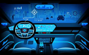
Smart Warnings: LLM-enabled personalized driver assistance
Read more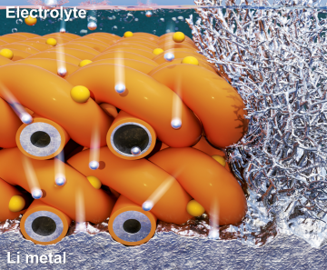
Extending the lifespan of next-generation lithium metal batteries with water
Read more
Professor Ki-Uk Kyung’s research team develops soft shape-morphing actuator capable of rapid 3D transformations
Read more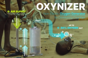
Oxynizer: Non-electric oxygen generator for developing countries
Read more