KAIST
BREAKTHROUGHS
Research Webzine of the KAIST College of Engineering since 2014
Spring 2024 Vol. 22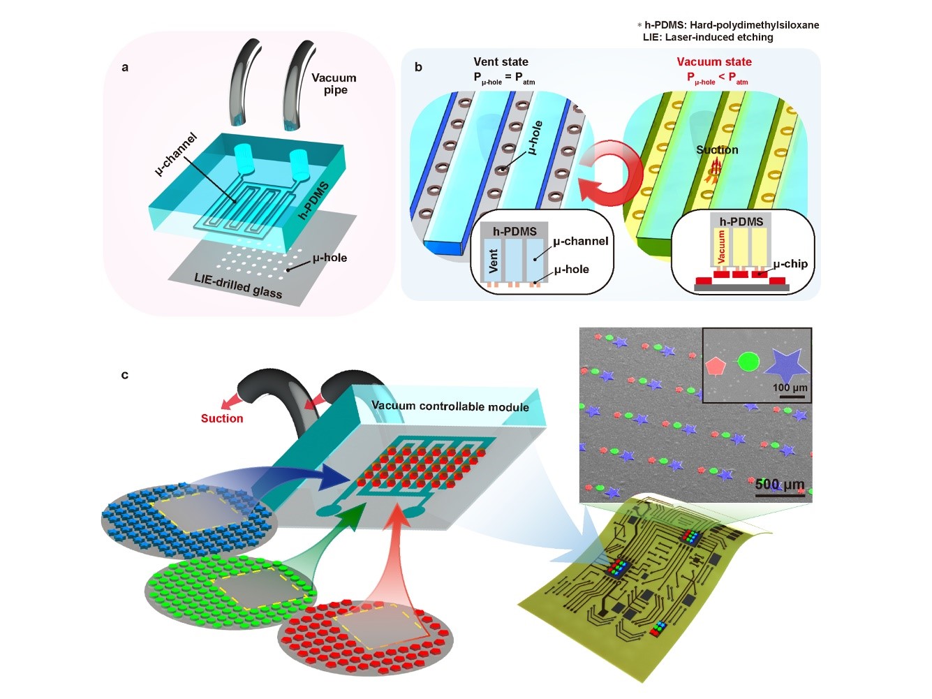
A KAIST research team led by Professor Keon Jae Lee demonstrates the transfer printing of a large number of micro-sized inorganic semiconductor chips through the selective modulation of micro-vacuum force.
MicroLEDs are a light source for next-generation displays that use inorganic LED chips with a size of less than 100 μm. MicroLEDs have attracted a great deal of attention due to their superior electrical/optical properties, reliability, and stability compared to conventional displays such as LCD, OLED, and QD. To commercialize microLEDs, transfer printing technology is essential for rearranging microLED dies from a growth substrate onto the final substrate with a desired layout and precise alignment. However, previous transfer methods still have many challenges such as the need for additional adhesives, misalignment, low transfer yield, and chip damage.
Professor Lee’s research team has developed a micro-vacuum assisted selective transfer printing (µVAST) technology to transfer-print a large number of microLED chips by adjusting the micro-vacuum suction force. The key technology relies on a laser-induced etching (LIE) method to form 20 μm-sized micro-hole arrays with a high aspect ratio on glass substrates at a fabrication speed of up to 7,000 holes per second. The LIE-drilled glass is connected to the vacuum channels, controlling the micro-vacuum force at the desired hole arrays to selectively pick up and release the microLEDs. The micro-vacuum assisted transfer printing accomplishes a higher adhesion switchability compared to previous transfer methods, enabling the assembly of micro-sized semiconductors with various heterogeneous materials, sizes, shapes, and thicknesses onto arbitrary substrates with high transfer yields.
Professor Keon Jae Lee said, “The micro-vacuum assisted transfer provides an interesting tool for large-scale, selective integration of microscale high-performance inorganic semiconductors. Currently, we are investigating the transfer printing of commercial microLED chips with an ejector system for commercializing next-generation displays (Large screen TVs, flexible/stretchable devices) and wearable phototherapy patches.”
The study titled “Universal selective transfer printing via micro-vacuum force” was published in Nature Communications on November 26th, 2023. (DOI: 10.1038/S41467-023-43342-8)
Title: Entire process including LIE and µVAST
Vimeo link: https://vimeo.com/894430416?share=copy
Most Popular
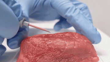
An intravenous needle that irreversibly softens upon insertion by body temperature
Read more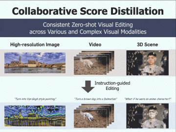
Consistent visual editing of complex visual modalities: videos and 3D scenes
Read more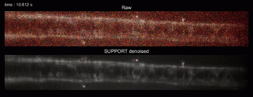
SUPPORT enables accurate optical readout of voltage signals in neurons
Read more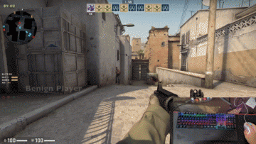
AI for detecting aimbots in FPS games
Read more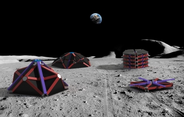
Origami-based deployable space shelter
Read more