KAIST
BREAKTHROUGHS
Research Webzine of the KAIST College of Engineering since 2014
Spring 2024 Vol. 22Clocking chips with light pulses: Cleaner signals and lower heat dissipation

A novel laser-based technology can generate and distribute electronic clock signals within semiconductor chips with femtosecond (10-15 second) precision timing and low heat dissipation, which have been challenging to achieve with conventional approaches.
As the performance of semiconductor chips has improved dramatically in recent years, the need for more precise and accurate timing inside chips has also become more critical. However, the necessity for a large number of clock drivers in a clock distribution network (CDN) to distribute clock signals within a chip not only impairs the timing performance but also causes on-chip thermal problems. As a result, both jitter (random variation in clock arrival time) and skew (spatial variation in clock arrival time) have been limited to several to tens of picoseconds.
A team of engineers from KAIST and Korea University, led by Prof. Jungwon Kim of KAIST, has developed a new optical method that employs an optical frequency comb source with sub-femtosecond timing jitter as the master clock to overcome this challenge. The light pulses produced by the optical frequency comb are converted into photocurrent pulses by high-speed photodiodes, and the CDN, which are on-chip metal-mesh structures, is charged and discharged to generate square-wave clock signals.
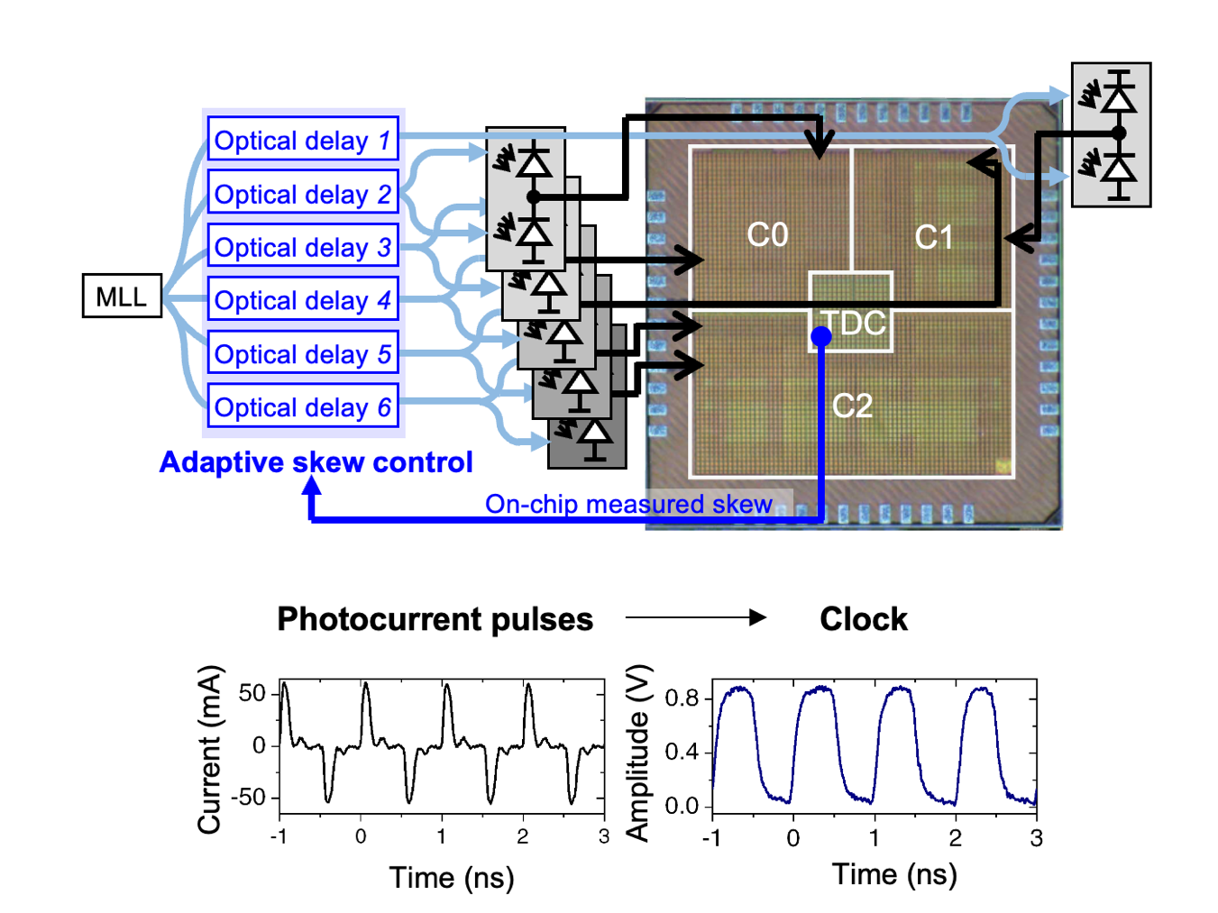
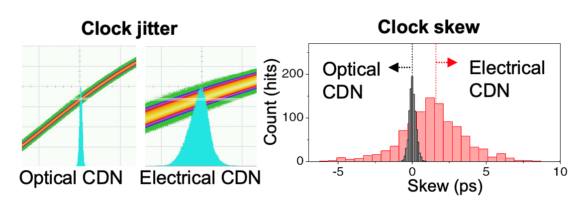
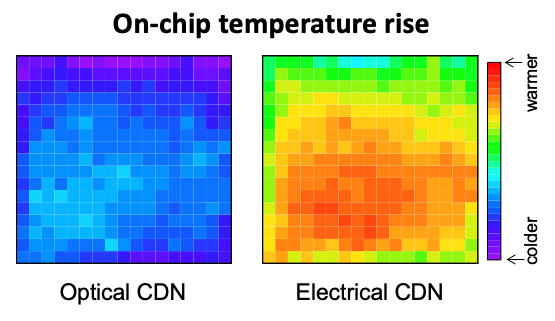
This method, in particular, allows the clock to be disseminated throughout the chip by eliminating the clock drivers and only using the driver-less metal mesh structures, which not only improved timing performance but also significantly reduced heat dissipation in the clock distribution. As a result, both jitter and skew were reduced to less than 20 femtoseconds, which is less than one-hundredth of a typical timing performance of electronic CDNs. In addition, on-chip power consumption and heat dissipation in clock distribution were also reduced to less than one hundredth of typical performances of conventional methods.
"We believe that this new method will find applications where both better timing and lower heat dissipation matter, such as 3D-stacked ICs with high-speed I/Os," Prof. Kim mentioned. “For more widespread applications of the demonstrated method, further development in chip-scale femtosecond lasers and on-chip optical amplifiers will be critical, and we are currently working on these techniques.”
The paper entitled “Femtosecond-precision electronic clock distribution in CMOS chips by frequency comb-extracted photocurrent pulse injection,” co-authored by PhD student Minji Hyun and Professor Hayun Chung’s group of Korea University Sejong Campus, was published in Nature Communications. This work was also featured in Research Highlights of May 2023 issue of Nature Electronics (entitled “Chips with a pulse”).
Most Popular
An intravenous needle that irreversibly softens upon insertion by body temperature
Read more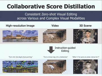
Consistent visual editing of complex visual modalities: videos and 3D scenes
Read more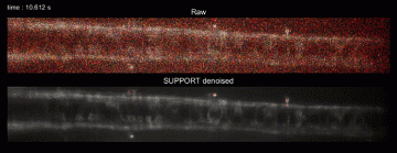
SUPPORT enables accurate optical readout of voltage signals in neurons
Read more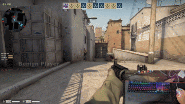
AI for detecting aimbots in FPS games
Read more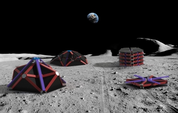
Origami-based deployable space shelter
Read more