KAIST
BREAKTHROUGHS
Research Webzine of the KAIST College of Engineering since 2014
Spring 2025 Vol. 24Plastic straw: The future of high-speed short-reach interconnects
A cost- and power-effective all-electrical-domain wideband waveguide solution has been developed for next-generation high-speed short-reach communication links
Article | Spring 2017
Professor Hyeon-Min Bae of the Electrical Engineering Department at the Korea Advanced Institute of Science and Technology (KAIST) demonstrated a cost- and power-effective all-electrical-domain wideband waveguide solution, referred to as an “E-TUBE.” This new interconnect scheme for next-generation high-speed input/output interfaces will be attractive to parties interested in high throughput links including, but not limited to, 100G/400Gbps chip-to-chip communications.
For decades, conductor-based electrical interconnects have been widely adopted for various wireline communication systems owing to the interconnect’s cost/power efficiencies. However, the skin effect, caused by electromagnetic induction, imposes a fundamental limitation on the channel bandwidth, in turn limiting the throughput-distance product, 100 Gbps/m. As such, it is generally believed that optical interconnects will eventually replace high-speed electrical interconnects in the foreseeable future.
Nevertheless, the widespread use of optical interconnects is severely challenged by the overwhelming replacement cost. The requirement of high-precision manufacturing for the electrical-to-optical and optical-to-electrical conversion process places an economic barrier in satisfying the market demand. Given the barriers, a cost-effective solution should be proposed to replace conventional conductor-based interconnects in high-speed, high-volume, short-reach communication links.
The figure shows the overall E-TUBE interface. The E-TUBE is a dielectric waveguide clad in metal foil and is plugged directly into the printed circuit board (PCB). The RF signal is transferred through a PCB trace and is launched to the waveguide via a microstrip-to-waveguide transition (MWT) that suppresses the reflection occurring at the discontinuities between the E-TUBE and the microstrip line. The implementation of the E-TUBE is based on a standard laminated printed circuit board (PCB) process and a low-precision manufacturing process, which is suitable for low-cost mass production.
The E-TUBE has nearly 20-GHz bandwidth over the V band and exhibits a frequency-independent insertion loss. The frequency-independent loss-profile of the E-TUBE does not require complex equalizers commonly used in conductor-based interconnects, and this lowers the power budget of an overall link.
The huge tolerance of coupling imperfection enables the usage of low-cost connectors, and the high bending tolerance enables the deployment of the E-TUBE to diverse applications. The E-TUBE is a promising solution for next-generation short-reach high-speed communication links in data centers such as the ultra-short-reach active optical cable link and the backplane links. In addition, E-TUBE would be attractive to high-end display interfaces such as a link between an ultra-thin UHD TV and external video sources.

Most Popular

When and why do graph neural networks become powerful?
Read more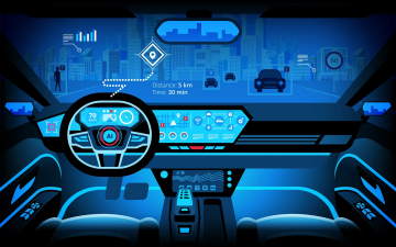
Smart Warnings: LLM-enabled personalized driver assistance
Read more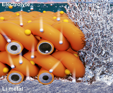
Extending the lifespan of next-generation lithium metal batteries with water
Read more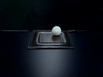
Professor Ki-Uk Kyung’s research team develops soft shape-morphing actuator capable of rapid 3D transformations
Read more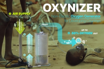
Oxynizer: Non-electric oxygen generator for developing countries
Read more